REV. 0
4
ADM1070
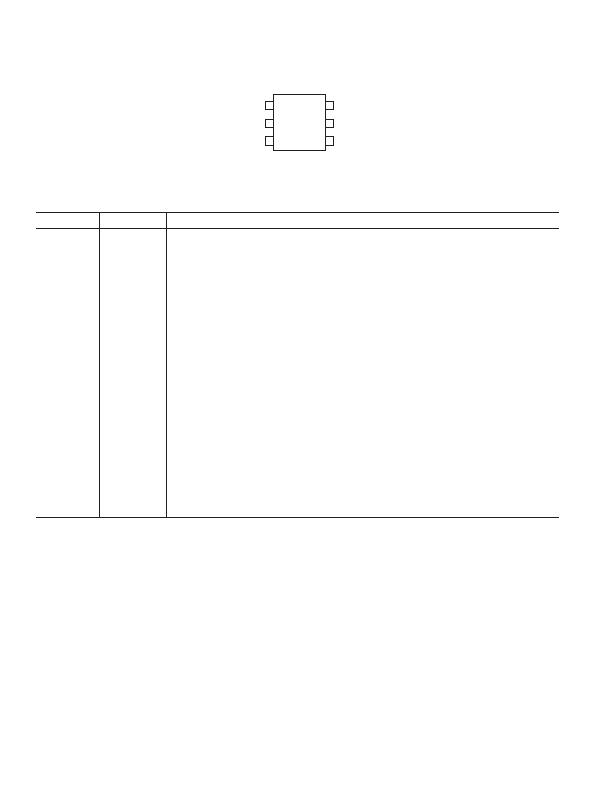
PIN CONFIGURATION
TOP VIEW
(Not to Scale)
6
5
4
SENSE
V
IN
GATE
UV/OV
TIMER
ADM1070ART
1
2
3
V
EE
PIN FUNCTION DESCRIPTION
Pin No.
Mnemonic Function
1
SENSE
Connection to External FET Source Voltage. A sense resistor is connected in the supply path
between the SENSE Pin and V
EE
, and the voltage across this resistor is monitored to detect current
faults. This voltage is fed as an input to the linear current regulator. When it reaches 100 mV for
a specified period, t
ON
, the regulator reduces the gate voltage and drives the FET as a linear pass
device. If current monitoring is not required, this feature can be turned off by shorting the
SENSE Pin and V
EE
together.
2
V
EE
Device Negative Supply Voltage. This pin should be connected to the lower potential of the
power supply.
3
V
IN
Shunt Regulated On-Chip Supply, Nominally V
EE
+ 12.3 V. This pin should be current fed
through a dropper resistor that is connected to the higher potential of the power supply inputs.
4
TIMER
Allows User Control over Timing Functions by Determining Frequency of Oscillator. Fre-
quency set by connecting external capacitor to V
EE
. Tying pin directly to V
EE
causes oscillator to
default to internally set value.
5
UV/OV
Input Pin for Overvoltage and Undervoltage Detection Circuitry. The voltage appearing on the
UV/OV Pin is proportional to board supply and is determined by external resistors. When the
voltage on UV/OV falls below the undervoltage threshold of 0.86 V, the GATE Pin is driven low.
When the voltage appearing at the UV/OV Pin rises above the overvoltage threshold of 1.97 V,
the GATE Pin is also driven low. If the external resistor ratio of R1/R2 = 40 is used, then this
gives an operating range of 36 V to 77 V.
6
GATE
Output to External FET Gate Drive. Controlled by linear current regulator. The gate is driven
low if an overvoltage or undervoltage fault occurs or if a current fault lasts for longer than the
time, t
ON
. When in linear regulation, the GATE Pin voltage is controlled as part of the servo loop.
No external compensation is required. When the FET is fully enhanced and the load capacitance
has been charged, the GATE Pin reaches a high level of typically 12 V.
发布紧急采购,3分钟左右您将得到回复。
相关PDF资料
ADM1073ARU-REEL
IC CTRLR HOTSWAP -48V 14TSSOP
ADM4210-2AUJZ-RL7
IC CTLR HOTSWAP LV TSOT23-6
ADVFC32SH
IC CONV V/F F/V MONO TO100-10
FAN4800ASNY
IC CTLR COMBO PFC/PWM 16-DIP
FAN4800AUN
IC PWM/PFC CTLR COMBO 16-MDIP
FAN4800CUN
IC PWM/PFC CTLR COMBO 16-MDIP
FAN4802MY
IC PFC CTRLR AVERAGE CURR 16SOP
FAN4802SNY
IC CTLR PFC/PWM COMBO 16-PDIP
相关代理商/技术参数
ADM1070EB
制造商:AD 制造商全称:Analog Devices 功能描述:ADM1070 Hot Swap Controller Evaluation Kit Documentation
ADM1072
制造商:AD 制造商全称:Analog Devices 功能描述:Dual, USB 2.0 Full/Standby Power Controller with Supply Steering
ADM1072ARQ
制造商:AD 制造商全称:Analog Devices 功能描述:Dual, USB 2.0 Full/Standby Power Controller with Supply Steering
ADM1073
制造商:AD 制造商全称:Analog Devices 功能描述:Full-Feature −48 V Hot Swap Controller
ADM1073ARU
功能描述:IC CTRLR HOTSWAP -48V 14TSSOP RoHS:否 类别:集成电路 (IC) >> PMIC - 热交换 系列:- 产品培训模块:Lead (SnPb) Finish for COTS
Obsolescence Mitigation Program 标准包装:119 系列:- 类型:热交换控制器 应用:通用型,PCI Express? 内部开关:无 电流限制:- 电源电压:3.3V,12V 工作温度:-40°C ~ 85°C 安装类型:表面贴装 封装/外壳:80-TQFP 供应商设备封装:80-TQFP(12x12) 包装:托盘 产品目录页面:1423 (CN2011-ZH PDF)
ADM1073ARU-REEL
功能描述:IC CTRLR HOTSWAP -48V 14TSSOP RoHS:否 类别:集成电路 (IC) >> PMIC - 热交换 系列:- 产品培训模块:Obsolescence Mitigation Program 标准包装:100 系列:- 类型:热插拔开关 应用:通用 内部开关:是 电流限制:可调 电源电压:9 V ~ 13.2 V 工作温度:-40°C ~ 150°C 安装类型:表面贴装 封装/外壳:10-WFDFN 裸露焊盘 供应商设备封装:10-TDFN-EP(3x3) 包装:管件
ADM1073ARU-REEL7
制造商:Analog Devices 功能描述:Hot Swap Controller 1-CH -80V 14-Pin TSSOP T/R 制造商:Analog Devices 功能描述:FULL FEATURED -48V HOT SWAP CTRL'R I.C. - Tape and Reel
ADM1073ARUZ
功能描述:IC HOTSWAP CTRLR -48V 14-TSSOP RoHS:是 类别:集成电路 (IC) >> PMIC - 热交换 系列:- 标准包装:50 系列:- 类型:热交换控制器 应用:-48V 远程电力系统,AdvancedTCA ? 系统,高可用性 内部开关:无 电流限制:可调 电源电压:11.5 V ~ 14.5 V 工作温度:-40°C ~ 85°C 安装类型:表面贴装 封装/外壳:10-TFSOP,10-MSOP(0.118",3.00mm 宽) 供应商设备封装:10-MSOP 包装:管件